FDMA430NZ Overview
Description
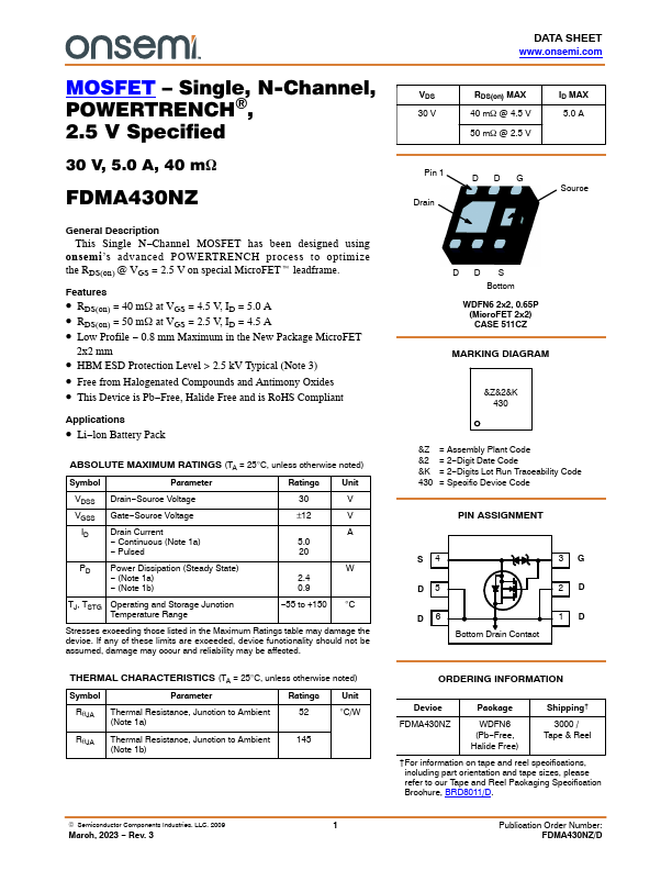
This Single N-Channel MOSFET has been designed using onsemi’s advanced POWERTRENCH process to optimize the RDS(on) @ VGS = 2.5 V on special MicroFETt leadframe.
Key Features
- RDS(on) = 40 mW at VGS = 4.5 V, ID = 5.0 A
- RDS(on) = 50 mW at VGS = 2.5 V, ID = 4.5 A
- 0.8 mm Maximum in the New Package MicroFET 2x2 mm
- HBM ESD Protection Level > 2.5 kV Typical (Note
- Free from Halogenated Compounds and Antimony Oxides
- This Device is Pb-Free, Halide Free and is RoHS Compliant